Home
What can you do with a Prusa 3D printer to help you make PCBs and Printed Circuits boards ?
I was very excited when I discovered the power of my Prusa 3D printer, and I immediately thought that I could add some more features to it. As I am also designing small electronics devices, I naturally searched for ways to help me in this task. I am proud to share with others my experiments and results on this topic. Other videos and printed files have already been published on this topic, but they are often missing some aspects, ( mainly the Software aspect ) and they do not really provide a complete guide.
You can also find some devices that will help making PCBs, but they are expensive, and will take some place within your home if you are doing this as a hobby. The main idea here is to use your existing PRUSA printer and add more features to it , without removing any 3D printer feature or quality. Last point, but not least, the entire project intends to provide low cost solutions ( once you already own a prusa 3D printer ! )
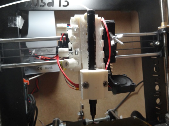
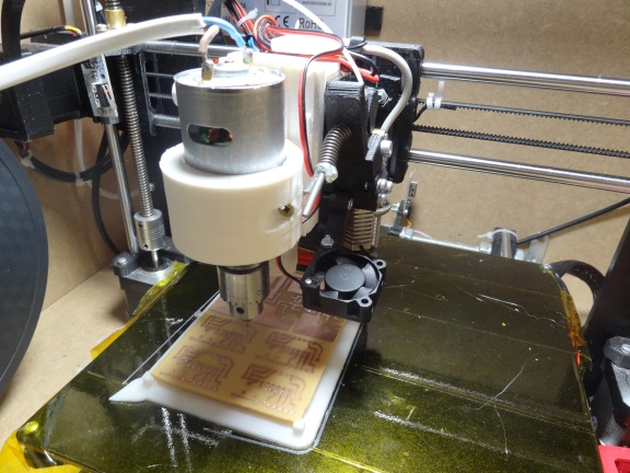
In order to make PCBs, i quickly realized that I would need additional tools mounted on the 3D printer ( pen, drill, Solderpaste dispensing, pick nplace.). This is why I designed the Teinturman’s tool holder, which allows to simply add tools to the printer, without removing or modifying the 3D printing feature.
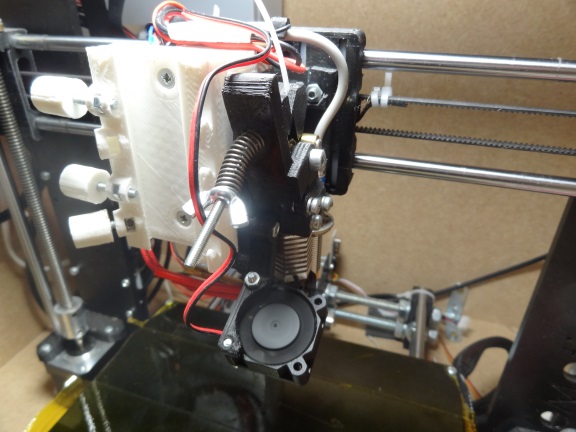
With a simple calibration procedure, it is then easy to move around any tool I need, with accurate positioning, via gcode files.
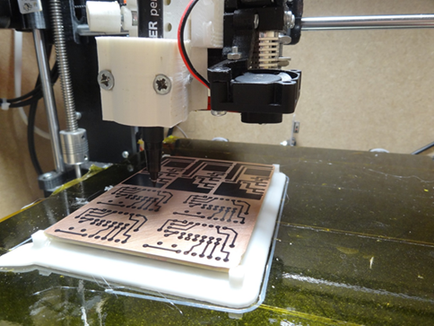
In order to ensure that the board I want to make is positioned precisely where it has to be on the printer bed, I found that the best approach was to print at a predefined position on the printer bed, a board support using the exact dimensions of the Copper board. The support is then precisely positioned where it has to be ( leave it where it is after printing ! ). From this point, i can generate gcode files to move the tools precisely , based on the fact that the copper board is positionned on this support which i know the exact coordinates on the bed. The only requirement is that the copper plate I want to use needs to have the exact Width and height dimensions that are declared into the PCB Software.
PCB Software? I searched for some freeware pcb design software, and after trying TCI, I finally went to DesignSpark7.2, which has a nice “Export to ODB++” function which dumps all the necessary information in readable text files. So, the principle is that you design your board using the DesignSpark7.2, software, then you export the ODB++files, and generate all the gcodes and 3D objects files that will help you building the PCB and Cis.
Easy isnt it?


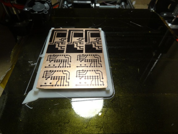
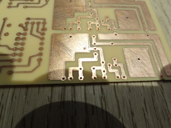
looking at the track with a microscope :

The etch resist pen process without insolation is not as good as using the etch resist pen, plus insolation process. the etching processis really up to what is your preferred etching method.
in both cases, you can draw directly on the PCB using the pcbfactory gcode files. The benefit here is that the process is quicker than using a laser print, thenan iron to transfer the toner to the pcb...
Also, using this method ensures that the tracks are written correctly aligned on the support, so it is then possible to use the gcode files to drill the pcb :
You can reproduce this experiment at low cost by following this complete guide :
You will need some printed parts ( stl provided for free) , some material you can find on eBay ( etch resist pen, drill motor (20€) ) and the software to generate the gcode ( 15€ payment is required in the download menu of this site. )
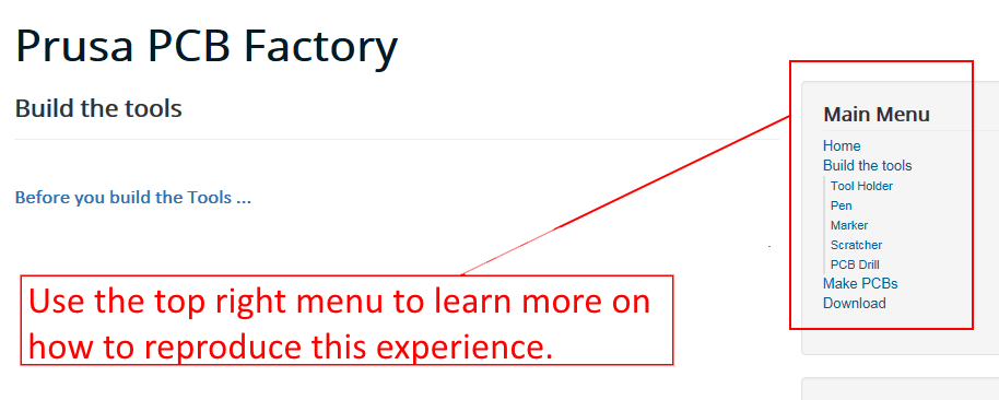
use the top right menu to read all the détails :
Click here to download the stl files to print the support Tools
You will need to Click here to Register before you can download the software
Click here to download the software.
So what are the end results before you learn how to do it :
-
Export a design spark PCB design, and convert it to a set of files that can be used on your 3D printer.
-
Draw precisely on the PCB with an etch resist pen , then etch with your preferred etching solution
- You can also use the etch resist marker and needle Scratch method
- You then can have your printer Drill the board using the automatically generated drill gcode ( one gcode file per drill diameter)
-
If you want to make many pcb of the same sort, you could test the 3D printed solder paste stencil
-
Build a Jig to maintain the board and its components while soldering the bottom face.